


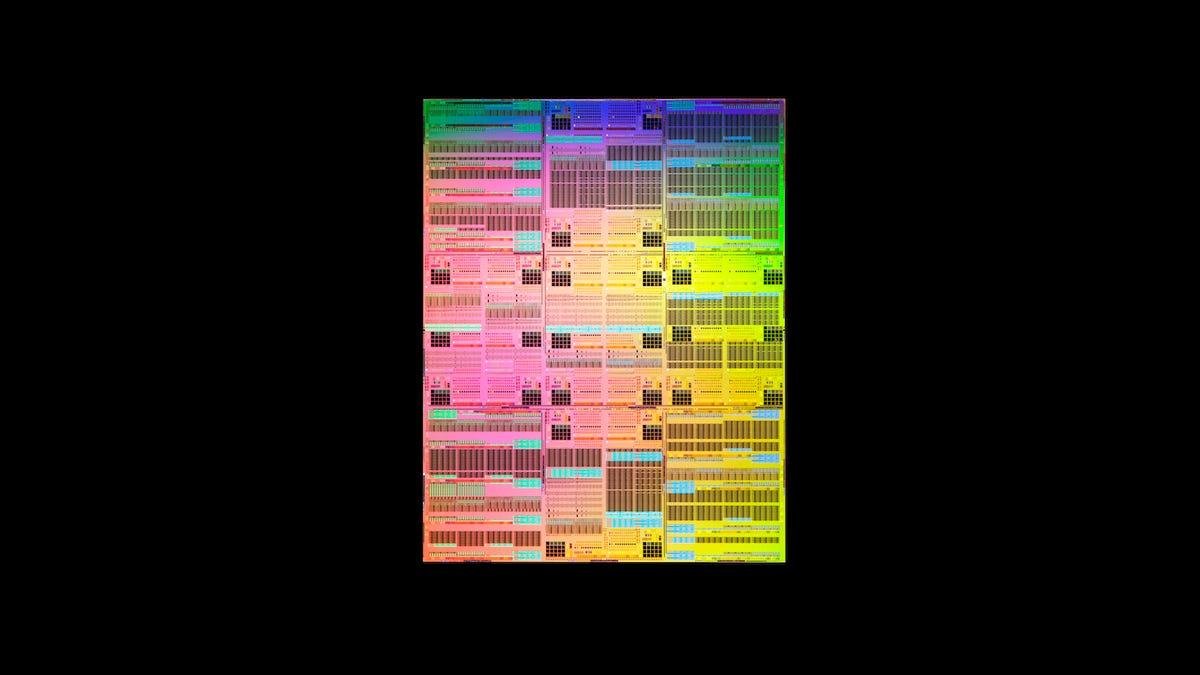


IBM on Thursday unveiled the first chip created using its latest semiconductor technologies, one that holds nearly 100 billion transistors in a fleck of hardware no bigger than your fingernail. Packing more transistors into a die the same size or smaller than previous generations is an essential part of increasing power efficiency and speed.
The new chip is 0.7 nanometers, smaller than IBM's two-nanometer chip that was first unveiled in 2021. But the circuitry of the new chip has been significantly adjusted. That older, larger process laid the transistors flat in what IBM Research called nanosheets, as CNET reported in 2021. Now, the new 0.7nm chip uses IBM's recently developed nanostack architecture, which stacks the nanosheets vertically.
IBM says the new architecture results in better performance. In the company's experiments, it found the new chip improved performance by up to 50% and energy efficiency by 70% compared to the 2nm version.
According to IBM, the nanostack architecture also allows for a 40% smaller die for SRAM -- static RAM is a type of memory that doesn't require a constant flow of electricity to store data, and because it's faster than DRAM, it's in high demand for AI applications.
An IBM researcher holds the company's sub-1nm node wafer.
IBMThe chip won't be ready to go for a while, though. IBM is still working with its manufacturing partner, Rapidus, a Japanese foundry (chip-making factory), to ramp up. IBM says it "sees a path to production" in five years, but the demand for energy-efficient computing hardware is only growing.
Chips like those designed by IBM, Nvidia, AMD and others are the backbone of the AI industry. As AI developers like OpenAI and Google race to build the most advanced models, they need massive amounts of energy, or compute, to train them. But that can take a lot of electricity, clean water and land to devote to data centers.
"Everyone demands more performance, but no one wants to pay for the bill for the power," said Huiming Bu, vice president of IBM semiconductor R&D. The new chip's energy efficiency "is a very critical component for AI," he said.
Creating more efficient hardware is a key piece of the AI-powered future that tech leaders envision. Current shortfalls in production capacity for memory, processors and other components have created shortages in the parts that are essential for any laptop or gadget you may want to buy. New research prototypes may help tech companies -- and everyone who uses their products -- get more bang for their buck in the future.
"Fundamentally, it comes down to, can we make transistors more efficient?" said Jay Gambetta, director of IBM Research. "This is a platform that can be customized, so our expectation is it's going to impact everything from the logic to the SRAM, and I expect we'll see, as this scales, more efficient, larger AI accelerators."